Ph.D. Applied Physics · Eindhoven

Martin Sas

Applied physicist. Twenty years taking sensing, photonics and advanced materials from the lab into production.

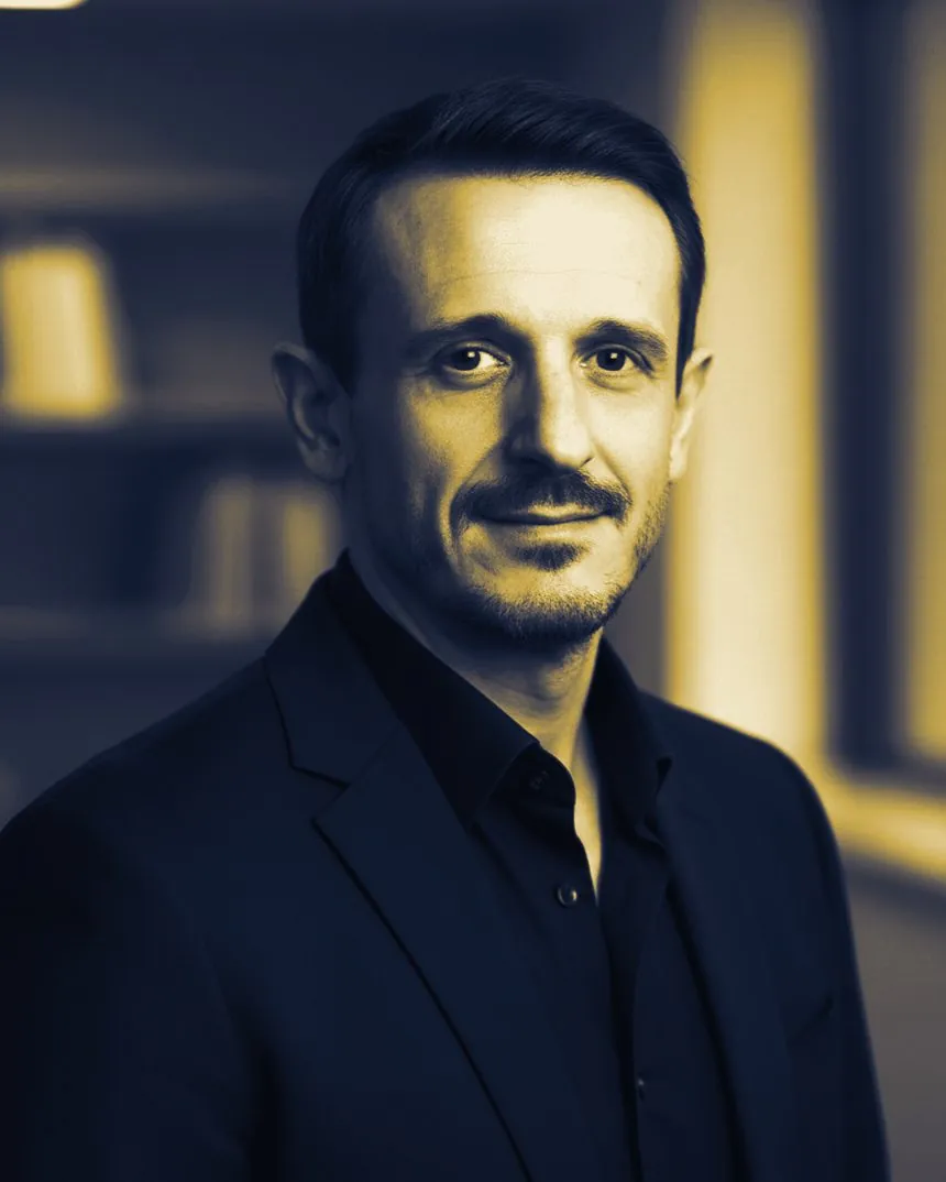
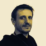
Portrait of Martin Sas

From physics to factory, in six steps

Worked on

  • PVD and CVD metallization
  • Laser Direct Structuring
  • SABIC T&I, 2015-2025

The thin film that conducts.

Where my work began at scale: PVD and CVD metallization, selective conductive patterning and Laser Direct Structuring. Atoms leave a target in a plasma and land one nanometre at a time.

Worked on

  • LiDAR design optimization
  • Optical sensing platforms
  • Research partner: CEA-Leti

Computation at the speed of light.

LiDAR design optimization, optical sensing and photonic integration. Light routed through waveguides instead of electrons through copper.

Trained in

  • Ph.D. scientific metrology, STU 2009
  • €1M metrology lab, built from scratch
  • Following: quantum sensing

Measuring the previously unmeasurable.

Metrology is where I trained: calibration, uncertainty budgets, validation. Quantum sensing is the next frontier of that discipline, and one I follow closely.

Building now

  • Agentic AI workflows
  • Local LLMs: Ollama, llama.cpp
  • Python, LangChain, Autogen

Where intelligence becomes infrastructure.

Agentic workflows and local LLMs, applied to engineering work: test automation, documentation and digital twins.

Delivered

  • 16 NPIs at SABIC
  • 4 sensor NPIs at Continental
  • EVT, DVT, PVT

From scattered parts to a system that works.

New products taken from proof of concept to production, every subsystem validated before it ships.

So that people, even the smallest, thrive.

It is why I am building a communication app for children with autism, and why UniPicto exists.

Where it converges.

Photonic AI, quantum sensing and assistive robotics, engineered into systems people can depend on.

The convergence of photonic AI, brain-computer interfaces, quantum sensing and assistive robotics is not abstract to me. It is the architecture of a future where people thrive.

Vision

These frontiers are not separate races. Light does the computing, quantum does the sensing, machines do the reaching and people do the deciding. I work where they meet, because that is where the future stops being a forecast and starts being engineered.

Mission

To close the distance between breakthrough and reality. The physics behind photonic compute, quantum sensing and embodied AI belongs in systems people can depend on: modelled before it is built, validated until it holds.
The evidence, not the optimism.

16 products to production, 5 patents, a €1M test centre, €6M platform revenue.

  • 16

    16 global NPIs across 4 platforms in 3 business units at SABIC, 2015-2025: ADAS sensing, RF shielding and EV thermal management.

    Before that, 4 automotive sensor NPIs at Continental, with 50% faster SOP readiness.

  • 20+

    Automotive at Continental and PSA, semiconductors at Freescale/NXP, advanced materials at SABIC: 2004 to 2025.

  • 5

    Electromagnetic materials, sensors and actuators. The granted patent (US12577392B2, 2026) covers composites with microwave shielding. The full list is under Record.

  • €1M

    An in-house electrical test and measurement centre at SABIC, built from scratch. It saves €1.5M OPEX a year, and a structured testing strategy cut validation cost by 60 to 80%.

  • €6M

    At Freescale/NXP, 2011-2015: embedded HW/SW and MEMS sensor platforms for 20+ Tier-1 and OEM accounts across the EU, US and APAC.

“I get thrilled when something works in a way nobody expected. And when it doesn't, I don't stop until it does.”

Martin Sas

What I work on.

Six domains, from physics modelling to validated production.

  • 20+ Tier-1 and OEM accounts

    RADAR, LiDAR and camera sensing, MEMS platforms, EV and power systems, from physics modelling to validated prototype.

    • ADAS sensing NPIs at SABIC, 2015-2025
    • MEMS sensor platforms at Freescale/NXP, 2011-2015
    • 4 automotive sensor NPIs at Continental, 2006-2011
  • Validation cost −60 to 80%

    Uncertainty budgets, calibration systems and EVT, DVT and PVT validation architecture.

    • Ph.D. in scientific metrology: SI calibration, laser interferometry, precision optical and thermal measurement (STU, 2009)
    • Built a €1M test and measurement centre at SABIC, saving €1.5M OPEX a year
  • CEA-Leti collaboration

    LiDAR design optimization and light-based sensing platforms for next-generation detection and compute.

    • Article on LiDAR design optimization in Photonics Spectra (2019)
    • Research collaboration with CEA-Leti
  • RF, EMI and triboelectric patents

    PVD and CVD metallization, selective conductive patterning, Laser Direct Structuring and plasma process development at SABIC.

    • Patents on RF-reflective thermoplastics, microwave-shielding composites and RADAR-absorbing materials
  • NXP, development cycles −30%

    MCU and SoC platforms, BLE, Wi-Fi and GPS, RF and EMI engineering across automotive, industrial and consumer IoT.

    • Technical contact for 20+ Tier-1 and OEM accounts at Freescale/NXP
    • Application notes and reference designs for major product launches
  • Python, LangChain, Ollama, Autogen

    Agentic workflows, LLM-assisted documentation, autonomous test pipelines and digital twins, built by someone who knows the physics underneath.

    • Local LLM inference with Ollama and llama.cpp
    • Edge AI: model quantization, pruning and distillation

The essential record.

Twenty years at SABIC, NXP and Continental, with education, patents and publications.

  1. 2025 to now

    Eindhoven, NL

    • A picture communication (AAC) app for children with autism
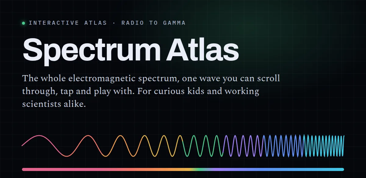
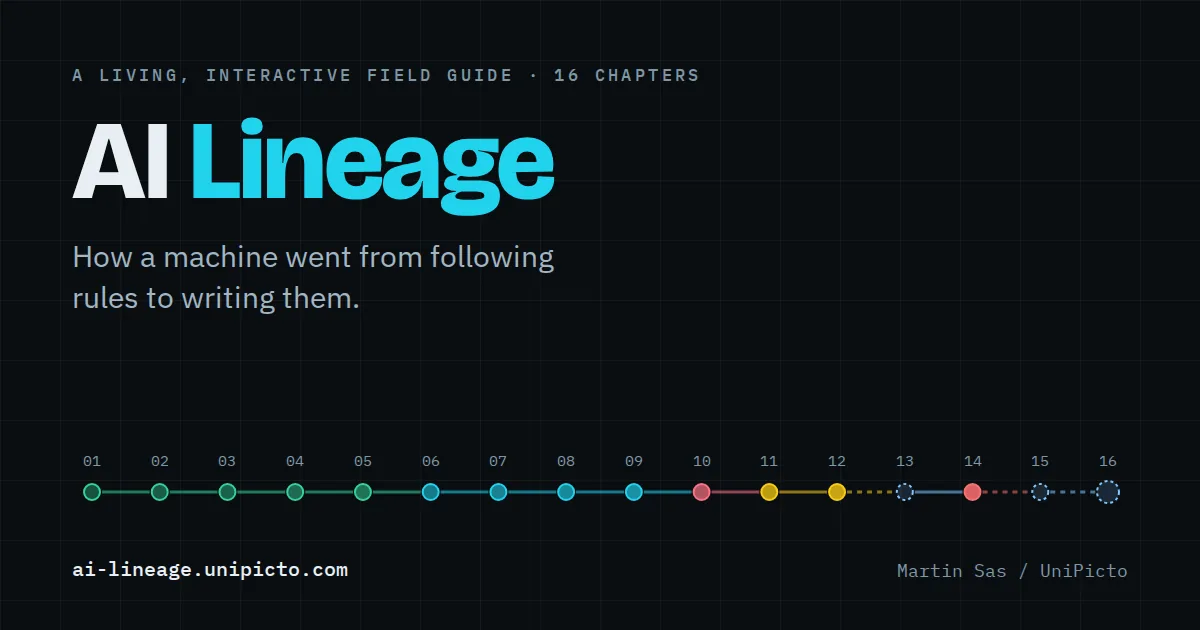
    • Interactive science sites under UniPicto: Spectrum Atlas, AI Lineage
    • Agentic AI workflows and local LLM inference (Ollama, llama.cpp)
  2. 2015-2025

    SABIC, T&I Centre, Bergen op Zoom, NL

    • 16 global NPIs across 4 platforms in 3 business units: ADAS sensing, RF shielding, EV thermal management
    • Built a €1M in-house electrical test and measurement centre, saving €1.5M OPEX a year
    • PVD and CVD thin-film metallization, selective patterning, LDS; validation cost −60 to 80%
    • Led 10+ specialists across EMEA, US and APAC; programme budgets up to €0.5M a year
  3. 2011-2015

    Freescale, now NXP, Rožnov, Czechia

    • Technical contact for 20+ Tier-1 and OEM accounts across the EU, US and APAC
    • €6M revenue across embedded HW/SW and MEMS sensor platforms; customer development cycles −30%
    • Application notes and reference designs for major product launches
  4. 2006-2011

    Continental, Frenštát, Czechia

    • Led a team of 3 to 5 FTE on automotive sensors, with FEM/CFD simulation and validation testing
    • 4 NPIs with 50% faster SOP readiness; €0.6M budget; prototyping cost −20%
  5. 2004-2006

    ATG Technologies, PSA Peugeot Citroën, Bratislava, Slovakia

    • Projects and a quality analysis team (5 FTE) across automotive and industrial operations

Education

Ph.D. Applied Physics, scientific metrology
STU, 2009
M.Sc. Mechanical Engineering, fluid physics
STU, 2001

Patents, 5 filed

RF-reflective thermoplastics
EP, lead inventor

Selected publications

Thermoplastic Faraday cage
Interference Technology, 2021
Circuit materials for ADAS
EE Times, 2020
LiDAR design optimization
Photonics Spectra, 2019

Research partners

Fraunhofer, CEA-Leti, KAUST, TU/e, Holst Centre

Languages

Slovak and Czech C2, English C1, German and French B1, Dutch A2

View CV

Current work.

A picture communication app for children with autism, and two interactive science sites.

All projects on unipicto.com

Let's compare notes.

Sensing, metrology, photonics or AI in engineering: if it is on your mind, write to me.